DC DC Converters
I wanted DC to DC converters for my solar powered wireless sensors - the requirements of these include a maximum current of 10 mA, high efficiency, operation at currents as low as one microamp and construction from standard very low cost parts.
Building converters is folly, since lots are available from major semiconductor companies with efficiencies of 90% which simple designs will never match - even if there are many home made converters with efficiencies of over 100% exhibited on You Tube. My aim is to discover how efficient the circuits below can be made.
Two transistor boost converter
Usually the output voltage is taken between the lower side of the input voltage and the inductor - this means the output voltage will never be (much) less than the input. Current can flow through the inductor directly from input (right) to output (left). The voltage added by the input supply in this arrangement is obtained at as high an efficiency as possible. This explains why it can be observed that with the output voltage close to the input voltage efficiency is high and as the output voltage increases efficiency decreases.
It is possible to take the output from between the high side of the input voltage and the inductor. In this configuration the output voltage can go down to zero. This might be described as a buck-boost converter.
Download
The circuit can be in two states when working.
- On - both transistors conducting, current in the inductor L1 increasing.
- Off - both transistors not conducting, current in the inductor decreasing. When the rate of change of current reverses (from increasing to decreasing) the voltage across the inductor also reverses. This is the situation in which the voltage is boosted. When the voltage across the inductor is reversed it is added to the positive side of the power supply, meaning any such voltage is an increase over the input.
Transitions repeatedly occur between the two states. The circuit is biased so that initially it is in the On state.
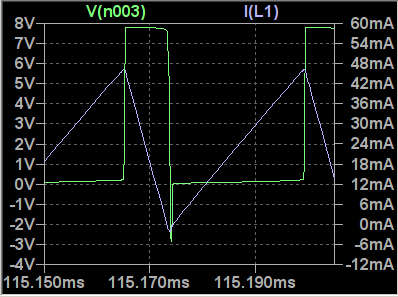
The blue curve shows the current through the inductor. The green curve is the voltage at the collector of Q2. During the upward slope of the current curve, Q2 is turned on and its collector voltage is close to zero. When Q2 is turned off the current slopes downward and the voltage is that of the boost converter output minus the input voltage.
The slope of the current curve is controlled by the equation for an inductor V = - L dI/dt. For the upward slope V is the power supply voltage (2 V here). The inductor is 1 mH, and the current gradient should be 2/0.001 = 2000 mA/ms. During the downward slope the voltage is that of the output 8 V minus 2V, giving a gradient of 6/0.001 = 6000 mA/ms.
Given the maximum current Imax, input voltage Vi and output voltage Vo. The period of oscillations is:
t = Imax/(Vi/L)+Imax/((Vo-Vi)/L) = Imax L(1/Vi+1/(Vo-Vi))
Predicting a frequency of around 30 KHz. A smaller inductor, smaller maximum current, higher input or output voltage mean higher frequency.
The duty cycle is defined as the fraction of the period of oscillation that the circuit is in the On state.
D=(1/Vi)/(1/Vi+1/(Vo-Vi))=1/(1+Vi/(Vo-Vi)) which implies Vi/Vo=1-D.
The circuit can be looked at as a non-inverting amplifier. When the base of Q1 goes up, so will the collector of Q2. They're connected by the capacitor C1 giving positive feedback. Oscillation results. Transitions between the On and Off states can be the result of C1 charging up and the circuit returning to its static bias state. This is not necessarily what happens.
Thinking about the transitions from the On state to Off. In the On state the collector of Q2 is close to zero volts. The base of Q1 has been pulled down via C1 which is charging up. However when C1 has charged the static bias position will be reached which by design still has Q1 turned on. One of two things happens either the current through Q1 is then not sufficient to keep Q2 saturated or the current in the inductor will continue to increase until this is true. When this happens the collector voltage of Q2 will rise, this rise is fed back to the base of Q1 via C1 reinforcing the increase in Q2 collector voltage. It is the rise in the voltage of Q2's collector due to the increasing current which causes the transition.
Now looking at the Off to On transition, in the Off state the voltage at the collector of Q2 is above the positive power supply voltage (due to the inductor) and C1 has pulled the base of Q1 high turning it off. One possibility is that C1 charges and the base of Q1 returns to the static bias position turning Q1 and Q2 back on. Another is that the current through the inductor will decrease to zero at which point the voltage across it will also go to zero, C1 then takes the base of Q1 down turning it on. At first the base of Q1 may be dragged down far enough for a substantial current to flow and C1 rapidly to charge.
Picking the various time constants selects which of the various possibilities occurs and how well the circuit performs.
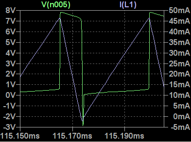
Here the blue curve is the current in L1 and the green curve is the voltage at the base of Q1.
One source of inefficiency is the diode D1. I often used a BAT85 which has a measured forward voltage of around 0.35 V; using an 1N5819 or SS14 this is 0.25 V. Supposing the circuit is supplying 5 V at 10 mA, 50 mW. The duty cycle is 3/5, the average current through the diode is then 10 mA * 5/2 = 25 mA, power loss 6 mW (or 8 mW for the BAT85). Immediately the efficiency is reduced to below 90% (or 85%) regardless of what the rest of the circuit does. This applies to any circuit which uses a diode in this way, including the simpler chips.
The BAT85 has a reverse leakage current of 0.1 μA whilst the other diodes are around 2 μA. Which means there's trade off regarding when power is wasted.
Another source of wasted power is the resistance of the inductor. The 4.7 mH inductor I set off using (see the photo below) has a resistance of 22 Ω. Putting 10 mA through that would use 2.2 mW. Added to the 8 mW lost in the diode, efficiency is down to 80%. I ended up using the Coilcraft DT3316P-105MLB which is 1 mH with 1 Ω resistance. The cheap resistor style inductors work OK, but not quite as efficiently. LT spice predicts an efficiency of 83% for the circuit.
Looking at the static bias of the circuit. Q1 is set up as the classic common emitter amplifier, with an emitter resistor and potential divider base bias. This should make results for Q1 predictable and less dependent on the parameters of individual transistors. For Q1 to conduct the base voltage must be at least 1 Vbe below the positive power rail. Similarly for Q2 to conduct its base must be 1 Vbe above the negative rail and Q1's base voltage must be higher than this. Outside of these limits, decreasing Q1's base voltage increases the current flowing through R5 and into the base of Q2. A bigger base current for Q2 implies a bigger Imax above.
Eventually I devised the circuits below. They're the same but one is made with pnp transistors and the other with npn. They work with the buck-boost configuration and are regulated. One result is that output voltage will never exceed the voltage set. The output voltage can be bigger or smaller than the input. In LT spice efficiency is predicted to be around 80%, however in reality the pnp version achieved a creditable 70% whilst the npn version was a disappointing 55%. Standby current is around 30 μA.
NPN version. Click to see circuit diagram full size. R12 and R13 are replaced with a potentiometer to set the output voltage.

Download
PNP version. Click to see circuit diagram full size. R8 and R9 are replaced with a potentiometer to set the output voltage.

Download
Mark 1 solar powered wireless sensor boost converter
This has an efficiency of around 65%, and it will keep running when the output from the solar cell is as low as 10 μA. It does work (as if that proves anything). The inductor is 4.7 mH with a resistance of 22 Ω, one of the cheap ones that looks like an old style resistor.
Click images to show full size


Download
What on earth was I thinking of? I'd started by copying the "2-Transistor Joule Thief Circuit" on this page:
Talking Electronics
A Joule thief is a circuit which will boost the voltage of a nearly exhausted battery enough to run an LED. The classic design is a single transistor oscillator using a transformer to supply positive feedback. An explanation of that and the two transistor version can be found here:
Quantsuff's Advanced Joule thief circuits (broken link
available on the wayback machine)
There are 100's more examples on the web:
Watsons eblog - Comprehensive Joule Thief blog
Make a Joule Thief - Big Clive originator of the name 'Joule Thief'
Der LED-Spannungswandler
Joule Thief improvements
High efficiency regulated Joule thief
Joule Thief Single Cell LED Driver
Eco nightlight
Unhappy with the efficiency of the two transistor circuit, I looked at the programmable unijunction transistor (PUT) oscillator. I fiddled with the PUT oscillator and turned it into a boost converter. However after building it, I found that changing component values slightly led to better operation. The circuit when set up as above, does a few cycles as a PUT and then starts to oscillate like the two transistor Joule thief. Change the component values and it works like a PUT all the time, but it's not as efficient in that mode. Oscillation is maintained by the capacitance of the diode D2 when reverse biased. "Mark 1" refers to my first effort, there are plenty of "Joule thief meets solar cell" circuits on the web.
A Buck Converter
I copied:
The 2-transistor Black regulator Roman Black
changing it to reduce the power use. The result is below. When built it achieved an efficiency of 90% and a standby current consumption of 10 μA. R7 and R8 are replaced by a potentiometer which sets the output voltage. For sensors, most of the time the current use is around 1 μA and it would be good to turn off the converter and let the sensor run on the full voltage, R9 is a step in that direction. Only when the sensor is using a lot of power is the buck converter worthwhile.
Click to show full size

Download
David Pilling's Wiki
Set view